Table of Contents
Want to know what makes Apple’s iPad tick? Well wait no longer: thanks to the FCC and some analysis from the people over at iFixit, we now know what the internal guts of the iPad look like.
The Federal Communications Commission has publicly posted a series of images and documents sent to it by Apple — they are documents ranging from calibration tests to photos of the internal components. Apple requested that these pictures not be posted for 180 days, but clearly that request was denied.
iFixit used the opportunity to analyze not only the WiFi iPad, but the 3G version as well. They’re still posting the results of their analysis of the teardown, but here are some of the highlights:
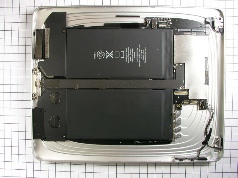
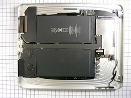
- The battery isn’t soldered into the iPad frame — it’s removable and replaceable by technicians in the same fashion as the iPhone
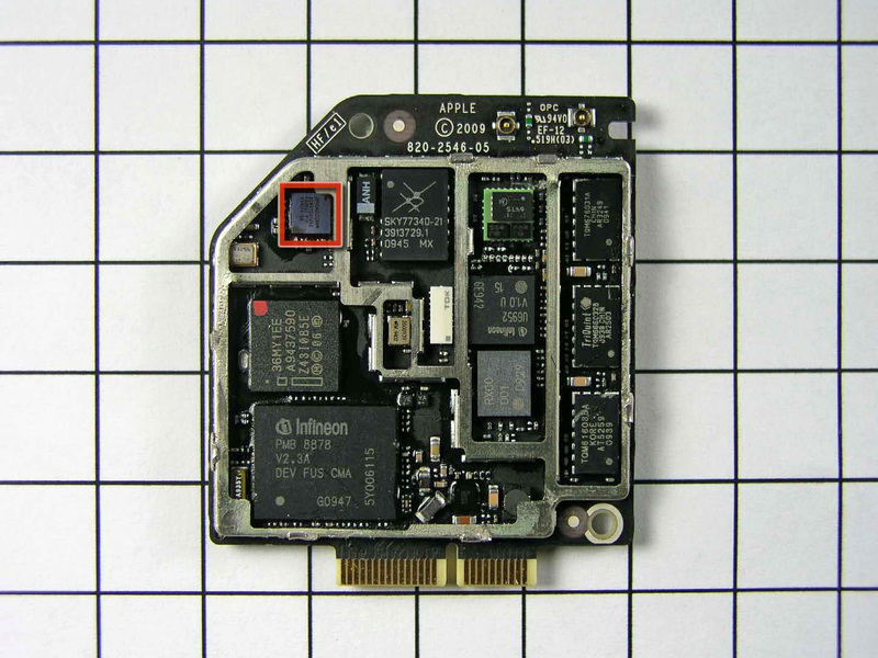
- Wi-fi and Bluetooth are integrated into a single board
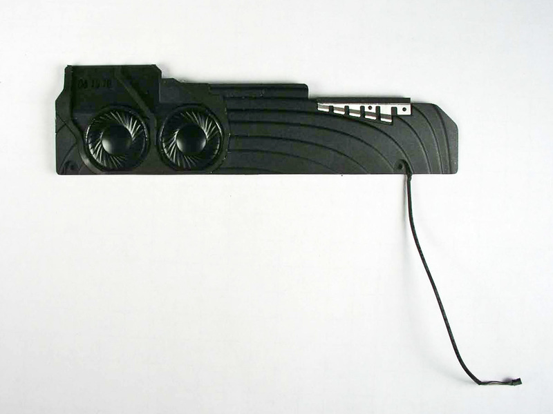
- Dual speaker system: aka stereo sound
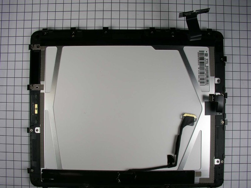
- The most expensive part of the iPad is likely the display assembly, specifically the in-plane switching technology and the LED backlighting. The display is most likely made by LG-Phillips
- The battery is a 24.8 watt-hour (6.5 Amp hour) battery. For context, the iPhone 3GS has a 4.51 watt-hour battery and the MacBook Air has a 40 watt-hour battery
- The iPad model’s number, according to the FCC, is A1337. Before you discuss Internet speak, the casing also sems to say that its model number is A1219, which would date the development cycle of the iPad all the way back to just after the beginning of development for the 1st gen iPod touch
If you want the nitty gritty details, we suggest checking out the full teardown, but we’ve included several of the FCC photos to whet your appetite.
iPad Teardown Photos